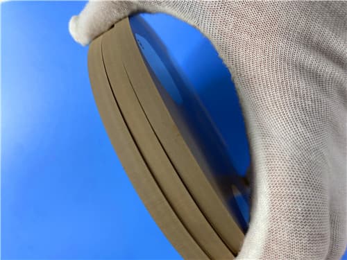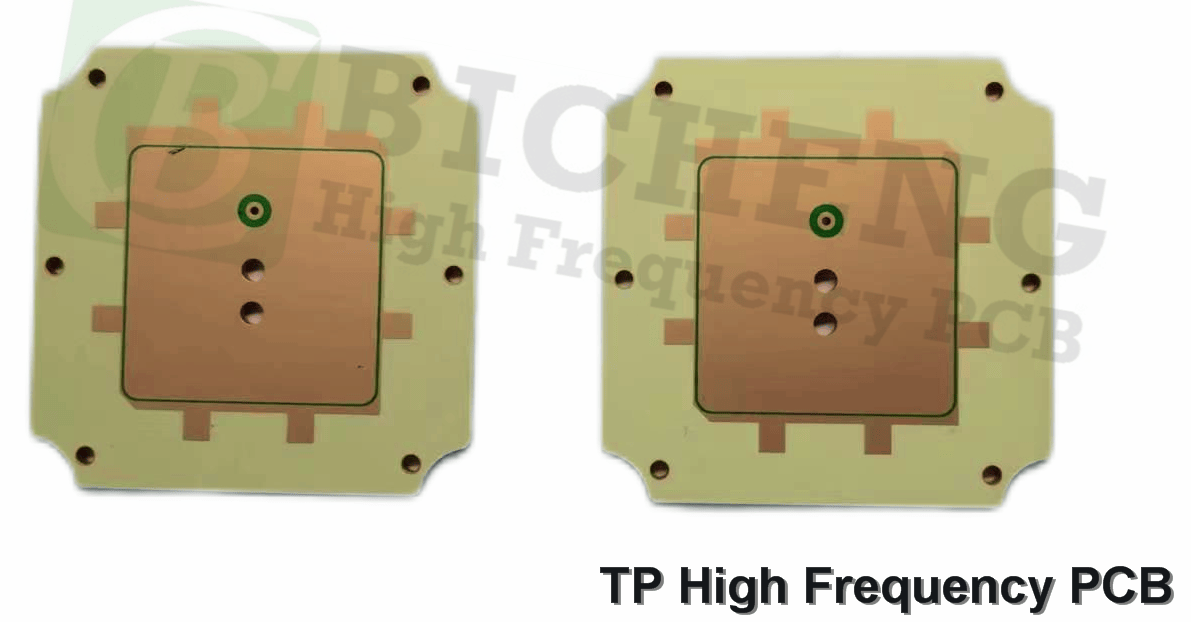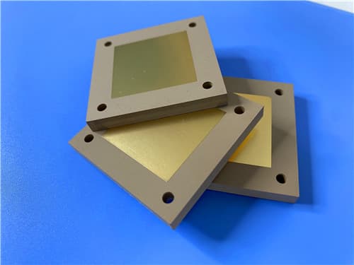
Wangling TP1600 2-Layer 0.9mm Pure Gold Plating PCB – High Dk Microwave Applications1. Introduction to Wangling TP1600 PCB TP1600 is a specialized high-frequency microwave composite dielectric copper-clad laminate (CCL). It belongs to the TP series, which uses a ceramic-filled polyphenylene oxide (PPO) resin matrix, no fiberglass reinforcement, formed via compression molding. The model number directly indicates its nominal dielectric constant of 16.0 (hence TP1600). The dielectric constant is precisely adjusted by modifying the ratio of ceramic to PPO resin. The production process is special, offering excellent dielectric properties and high reliability. TP material is a unique high-frequency thermoplastic material in the industry. The dielectric layer of TP series laminates is composed of ceramic and polyphenylene oxide (PPO) resin, without fiberglass reinforcement. The dielectric constant is precisely adjusted by modifying the ratio between ceramic and PPO resin. TP refers to non-clad smooth material, TP-1 refers to single-sided copper clad, and TP-2 refers to double-sided copper clad. This 2-layer rigid PCB is constructed entirely with Wangling TP1600 as the core material, making it ideal for miniaturized antennas, RF/microwave filters, couplers, resonant cavities, aerospace, defense, satellite payloads, and navigation (Beidou) applications.
2. Key Features of Wangling TP1600 PCB Dielectric constant (Dk/εr) of 16.0 ± 0.32 (16.0 ± 0.4 per data sheet) Dissipation factor (Df/tanδ) of 0.0012 at 5 GHz (0.0015 typical) TcDk (Temperature Coefficient of Dk) of -40 ppm/°C Z-axis CTE of 45-50 ppm/°C High Dk with low and stable loss for compact antennas, resonant structures, and high-frequency matching networks Minimal Df variation up to 10 GHz No fiberglass cloth: smooth surface, uniform electrical performance, avoids weave effect issues Radiation-resistant and low outgassing for aerospace, satellite, and military applications Thermal conductivity of 0.80 W/(m·K) Density of 2.76 g/cm³ Long-term operating temperature: -100°C to +150°C 3. Benefits of Wangling TP1600 PCB High Dk enables circuit size reduction for compact antenna designs Low and stable loss ensures excellent high-frequency performance No fiberglass reinforcement eliminates glass weave effect Smooth surface provides uniform electrical performance Easier machining than pure ceramics: drillable, turnable, grindable, etchable Reliable copper-dielectric adhesion compared to vacuum-deposited ceramic substrates Thermoplastic processing offers good yield and lower fabrication costs than alumina/AlN ceramics Radiation-resistant for space applications Low outgassing meets aerospace requirements 4. Wangling TP1600 PCB Construction Details
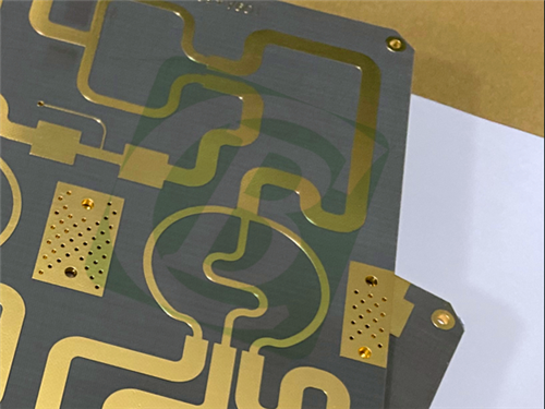
5. PCB Stackup (2-Layer Rigid Structure) Copper_layer_1 - 35 μm (1 oz) TP1600 Core - 0.8 mm (31.49 mil) Copper_layer_2 - 35 μm (1 oz) 6. PCB Statistics Components: 34 Total Pads: 56 Thru Hole Pads: 29 Top SMT Pads: 27 Bottom SMT Pads: 0 Vias: 34 Nets: 2 7. Primary Application Areas Miniaturized antennas RF/microwave filters, couplers, resonant cavities Aerospace, defense, satellite payloads, navigation (Beidou) High-frequency sensor modules requiring stable high-Dk performance Missile-borne and fuze applications 8. Quality Assurance Type of artwork supplied: Gerber RS-274-X Accepted standard: IPC-Class-3 Availability: Worldwide 9. Important Processing Notes No wave soldering permitted Reflow soldering max temperature ≤ 200°C (if used at all) Hand soldering preferred Material not suitable for 260°C thermal shock testing Not recommended for standard multilayer lamination (use low-Tg prepregs only if necessary, after feasibility review) Long-term use temperature: -100°C to +150°C (above 180°C may cause deformation, copper peeling, and electrical property changes) 10. Wangling TP1600 Ceramic-Filled PPO Laminate – Product Introduction TP1600 is a specialized high-frequency microwave composite dielectric copper-clad laminate (CCL). It belongs to the TP series, which uses a ceramic-filled polyphenylene oxide (PPO) resin matrix, no fiberglass reinforcement, formed via compression molding. The model number directly indicates its nominal dielectric constant of 16.0. The dielectric constant is precisely adjusted by modifying the ratio of ceramic to PPO resin. The production process is special, offering excellent dielectric properties and high reliability. TP material is a unique high-frequency thermoplastic material in the industry. The dielectric layer of TP series laminates is composed of ceramic and polyphenylene oxide (PPO) resin, without fiberglass reinforcement. The dielectric constant can be selected within the range of 3 to 25 according to circuit requirements, with common Dk values including 3.0, 4.4, 6.0, 6.15, 9.2, 9.6, 10.2, 11, 16, and 20. The material exhibits low dissipation factor with minimal variation up to 10 GHz. The material offers excellent radiation resistance and low outgassing, making it ideal for Beidou navigation, missile-borne, fuze, and miniaturized antenna applications. Copper-to-dielectric adhesion is more reliable than vacuum-deposited coatings on ceramic substrates. The material is easy to machine (drilling, turning, grinding, shearing, etching) – a significant advantage over ceramic substrates. PCB fabrication is convenient using standard thermoplastic processing methods, with high yield and much lower fabrication costs compared to ceramic substrates. Due to material characteristics, multilayer processing is generally not recommended. If multilayer processing is required, use low-temperature bonding films only after thorough feasibility review.
11. Features and Benefits Summary
12. Wangling TP1600 Data Sheet
13. Dielectric Constant Options (TP Series) TP series can provide dielectric constants from 3 to 25 as required, including: 3.0, 4.4, 6.0, 6.15, 9.2, 9.6, 10.2, 11, 16, 20. 14. Some Typical Applications Miniaturized antennas RF/microwave filters, couplers, resonant cavities Aerospace, defense, satellite payloads, navigation (Beidou) High-frequency sensor modules requiring stable high-Dk performance Missile-borne and fuze applications 15. Standard Thicknesses, Panel Sizes & Claddings Standard Thicknesses (Total thickness with copper or dielectric thickness – customer must specify)
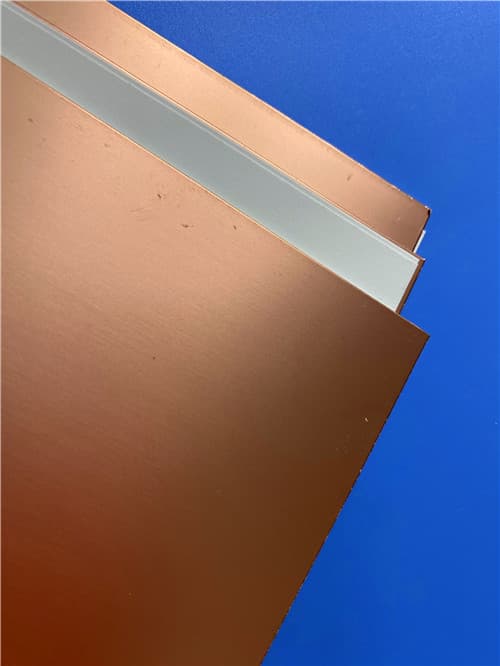
Note: Minimum thickness available is 0.5mm. Custom thicknesses available upon request. Copper Foil Options Copper foil type: ED copper foil Copper thickness: 0.018 mm, 0.035 mm Standard Panel Sizes
|
Get a Quick Quote
Fill in the form below and our engineers will reply within 24 hours with technical specifications and pricing for Wangling TP1600 2-Layer 0.9mm Pure Gold Plating PCB.